This tutorial on circuit board manufacturing is the first in a series of presentations on technical topics that will appear on our web page. Future updates will cover structural analysis of the car and eventually the most of the electrical and mechanical system of Monsoon.
On the Arizona Solar Racing Team, we make all our own circuit boards (at least for prototypes), mostly due to the cost of pro-made boards. However, it is pretty convienent to make them yourself, because you can have a working board in a day.
I've been refining the method we use for more than 6 years, and it is very reliable and easy. This method uses laser printed transparencies as a mask on pre-sensitized positive acting circuit boards (from GC Thorsen). Line widths down to less that 12 mil can be made this way (this is good enough for SSOP packages).
The first step is to create your circuit pattern, either
with a commercial program made for this purpose, or simply with a drawing
program like Adobe Illustrator or even something like Microsoft Paint (though
making the printed version the correct size may be difficult). I've make
boards both ways, but of course, the professional board programs make it much
easier.
As a simple example, here is an adaptor so you can use
the surface mount package SO-8 in a normal breadboard (the picture is not actual
size, but the pdf link will print actual size).
The next step is to print it on a laser printer on a transparency. The key
to this technique is to print it twice, to make the
dark areas dark enough. So print your pattern again, using the same transparency. Try
to align the transparency in the printer exactly the same way both times. A
misaligned printout will look like this:
It typically takes me two or three tries to get one that is perfect. I've had good success with the HP
LaserJet 6MP and the LaserJet 4MP. The LaserJet 3 almost never let me
print twice with good alignment. I would guess any 600dpi laser printer
will give good results with some practice. I've found it helps to let the
transparency cool before printing on it again.
The next step is to tape your transparency
onto a piece of glass. It is important to make sure the right side of the
transparency is facing the glass, otherwise your pattern will be mirrored on the
board. It is helpful if you print some text on or near the pattern so it
is easy to tell which side is which.
In a room that's not too brightly
lit, peel off the protective sheet from the circuit board, and align it with
your pattern. Place something flat on the back side of the board (like
another piece of glass) and clamp it together. I use large paper binder
clips for this (using these has an advantage you'll see later). Double
check your alignment and make sure that the pattern is not mirrored. Now
you are ready to expose! I keep the whole thing shielded from light until
I am outside and ready to go. I usually just put it inside a newspaper or
whatever's handy while I get setup outside. It is best to do your exposure
around noon, on a cloudless day. If it is partly cloudy, or much earlier
or later than say, 11 AM-2 PM, you will have to experiment with the exposure
time.
Now expose it to the sun for 1.5 to 2.5 minutes (depending on the light
conditions, how thick your glass is, weather, latitude, etc). Fortunately,
this process is not too sensitive to exact exposure time. Here in
Tucson, we're known for our strong sun and cloudless days. Two minutes
works well for me. You can use the levers on the binder clips to get your
board aligned perfectly normal to the sun by making the shadows of both clips
line up. When you are done exposing, wrap it up, and take it inside for
development.
The developer for the GC Tech positive acting boards I use is part number
22-226. This is basically a sodium hydroxide solution (no pun indended),
so you should keep it in a tightly closed container when you are not using it to
prevent the pH from changing. If you keep the developer in a tightly closed container it will
develop a lot of boards and last a long time.
Be sure you read, understand and follow the instructions on both the developer and the etchant solutions
before you begin. My instructions here are just a guideline, and are not intended to be a
substitute for the label instructions.
Place your exposed board in a plastic tray and pour in enough developer to
cover the board. You can speed things up and get a better pattern by
gently rocking the tray so fresh solution is washing over your board. In
just a few seconds you will see the pattern start to form, and within a couple
minutes the exposed areas will be completely washed away. You don't want
to overetch, but it is better to be sure the exposed regions are
completely
rinsed away. You can take the board out and wash it carefully
with water then give it a close up inspection to be sure. Be careful not to touch the
pattern with your fingers or anything else. It is easy to scratch it and that
will cause problems when we etch. When the pattern is finished developing, pour your
developer solution back into its container.
Before you start etching the board, it is a very good idea to put on some old
clothes, or wear an apron and gloves. The board etchant contains ferric
chloride which will permanently stain your clothes, or almost
anything else it touches, like your countertop.
The etchant works faster if it is warm. You can
warm the solution by flowing warm water over the bottle for a few minutes before
you use it (be sure to loosen the cap a little). It will still work fine
if you don't warm it though. Place your developed board into a plastic tray
and pour in the etchant. You will want to gently rock the tray frequently
during the etching to speed things up. Depending on how fresh your solution
is, how warm it is and how much you agitate the solution, the etching will take
from 10 minutes to more than an hour. You will have to
check the progress of your board. It is done when the copper is
completely gone from the exposed areas. It is helpful to
take the board out of the etchant and rinse it with water for better inspection. When the
board is done, rinse it thoroughly with plenty of water.
Finishing touches
Now you can start drilling all the holes for your leaded
parts. It is easiest to use a dremel for the small holes. The size of the holes
can be measured from the actual components, or read off the datasheets for that part.
Be careful not to drill larger than it needs to be. This can make soldering the lead to the pad
a little difficult.
Tips and tricks
Make your circuit traces as wide as possible. Though I've had success makes traces as narrow as 0.012", there
are often pinholes in the traces than can cause open circuits. This is especially true if the board is overexposed.
It is important to experiment with exposure time. Too much exposure causes the minor defects in the transparancy
to show up in your pattern. Of course, not enough exposure and the exposed areas will not be completly removed by
the developer, so the etching will not be able to remove the copper completely. This will cause short circuits at
worst, and large leakage currents as best.
I cannot emphasize enough the utility of placing text on your patterns. After your pattern is sandwiched between
the glass but before you go outside to expose, LOOK at the pattern and verify it
is on correct. It is way to easy to put the wrong side of the transparency towards the board, which would make
a mirror image of your pattern.
After you develop your pattern, inspect it carefully with a magnifying glass before etching. If there are scratches or holes
in the resist pattern, you can touch it up with a permanent marker. Permanent marker will resist the acid
etch remarkably well.
Don't forget to wear clothing protection, as well as eye and hand protection. The board etchant has ruined
more than a few of my shirts before I wised up.
After the etching is complete and you have rinsed and dried the board thouroughly, you can double check that
all the copper is removed by checking continutity between closely spaced parts of the board with a multimeter.
If there is no residual copper still on the board, you will see resistances greater than 30 Mohms
(the most I can measure with my meter) between closely spaced points on the board. This is only a fair test if
the board is dry.
The green photoresist can be easily removed with acetone (nail polish remover) or less easily with rubbing alcohol.
There is no need to buy the expensive resist stripper you may see in stores.
It is useful to make the hole sizes of your component pads the actual
size you will be drilling them, or a little smaller. This helps guide the drill bit when you drill so your
holes will be better aligned. You'll want to buy a wire drill index with sizes 61-80.
By Dr. Richard Workman
Arizona Solar Racing Team Alumnus
|
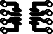
The pattern must be printed twice to be dark enough. It often takes several tries to get a good dark pattern
 |
The printed pattern is aligned with the board and sandwitched between two pieces of glass
 |
The pattern is exposed to the sun for 1.5 to 2.5 minutes. You can easily orient the board normal to the sunlight by aligning the shadows of the binder clip.
 |
Place the exposed board in a tray and add developer solution
 |
Soon, the pattern will begin to show on the board. Continue until the exposed areas are complete washed away.
 |
The fully developed board, ready for etching
 |
Put the board in a plastic tray and carefully pour in the etching solution.
 |
You can see the copper is removed near the upper
right side of this board, but the middle sill has copper. Back into the juice!
 |
Here is the fully etched board with no copper visible anywhere in the exposed regions.
 |
The holes are drilled to the right size for each
component with a dremel. Pay
attention! Driling the holes in slightly the wrong place can make it difficult to insert multileaded components like DIPs.
 |
If you
have more than one circuit on your board, it is
easiest to cut them out after drilling.
What? You don't have a band saw? A
hack saw works great too. Rough edges are easily filed.
 |
|